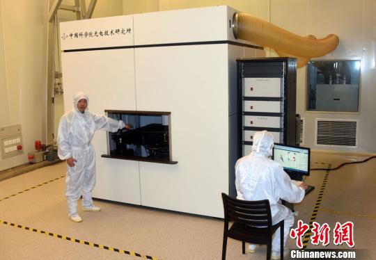
Yong Yang (left), deputy chief designer of Super-resolution Lithography Equipment Project of Institute of Optoelectronics, Chinese Academy of Sciences, introduces the successfully developed equipment. Sun zifa
Zhongxin. com, Chengdu, November 29th (Reporter Sun Zifa) — — The super-resolution lithography equipment project passed the acceptance test in Chengdu on the 29th. As one of the important achievements of the project, China scientists have successfully developed the world’s first ultra-resolution ultraviolet (i.e. 22nm @ 365nm) lithography equipment with the highest resolution, and formed a brand-new nano-optical lithography process route with completely independent intellectual property rights.
Researcher Luo Xiangang, director of the Institute of Optoelectronics of the Chinese Academy of Sciences and chief scientist of the super-resolution lithography equipment project, said that in 2012, the institute undertook the development task of super-resolution lithography equipment, a major national scientific research equipment project. After nearly seven years of hard work, without foreign mature experience to learn from, the project team broke through key technologies such as high uniformity lighting, super-resolution lithography lens, nano-resolution focusing and gap measurement, and ultra-precision, multi-degree-of-freedom stage and control. The development of the first UV super-resolution lithography equipment with the highest resolution in the world is completed. It uses a light source with a wavelength of 365 nm, and the maximum line width resolution of a single exposure reaches 22 nm (about 1/17 exposure wavelength). On this basis, the project team also combined with the supporting processes such as high aspect ratio etching and multiple patterns developed by the super-resolution lithography equipment project to realize the processing of feature size patterns below 10 nanometers.
The first ultra-violet super-resolution lithography equipment with the highest resolution in this world is developed based on surface plasmon super-diffraction, which breaks the traditional route pattern that the resolution of traditional optical lithography is limited by the wavelength of light source and the numerical aperture of lens, and forms a brand-new technical route from principle, equipment to process, with completely independent intellectual property rights, and provides manufacturing tools for the leap-forward development of revolutionary strategic fields such as metamaterials/hypersurfaces, third-generation optical devices and generalized chips.
Acceptance experts believe that all technical indicators of the super-resolution lithography equipment successfully developed by Zhongke Optoelectronics meet or exceed the assessment indicators specified in the implementation plan, and the key technical indicators have reached the international leading level in the field of super-resolution imaging lithography. In principle, the project breaks through the diffraction limit of resolution, establishes a new research and development route of high-resolution and large-area nano-lithography equipment, bypasses the technical intellectual property barrier of foreign high-resolution lithography equipment, realizes the innovation of China’s technological source, and develops super-resolution lithography equipment with independent intellectual property rights and controllable technology, which is also the first ultra-violet super-resolution lithography equipment with the highest resolution in the world.
At the same time, a series of nano-functional devices, including large-aperture thin film mirror, superconducting nanowire single photon detector, Cherenkov radiation device, biochemical sensor chip, super-surface imaging device, etc., have been prepared by using the successfully developed super-resolution lithography equipment, which verifies the processing ability of the nano-functional devices of the equipment and has reached the practical level.
The super-resolution lithography equipment project of Zhongke Optoelectronics Institute has published 68 papers, and at present, it has been authorized 47 national invention patents and 4 international patents, and has trained a super-resolution lithography technology and equipment research and development team. Luo Xiangang said that the Institute of Optoelectronics of the Chinese Academy of Sciences will further increase the research and development, popularization and application of functional diversification of super-resolution lithography equipment to promote the development of related fields in the country.
关于作者